- 您现在的位置:买卖IC网 > Sheet目录3891 > PIC18C801T-I/L (Microchip Technology)IC MCU ROMLESS A/D PWM 84PLCC
2001 Microchip Technology Inc.
Advance Information
DS39541A-page 113
PIC18C601/801
9.5
PORTE, TRISE and LATE
Registers
PORTE is an 8-bit wide, bi-directional port. The corre-
sponding data direction register is TRISE. Setting a
TRISE bit (= 1) will make the corresponding PORTE pin
an input (i.e., put the corresponding output driver in a
Hi-Impedance mode). Clearing a TRISE bit (= 0) will
make the corresponding PORTE pin an output (i.e., put
the contents of the output latch on the selected pin).
Read-modify-write operations on the LATE register
reads and writes the latched output value for PORTE.
PORTE is an 8-bit port with Schmitt Trigger input buff-
ers. Each pin is individually configurable as an input or
output. PORTE is multiplexed with several peripheral
functions (Table 9-9).
PORTE is multiplexed with the system bus and is avail-
able only when the system bus is disabled, by setting
EBDIS bit in register MEMCON. When operating as the
system bus, PORTE is configured as the high order
byte of the address/data bus (AD15:AD8), or as the
high order address byte (A15:A8), if address and data
buses are de-multiplexed.
EXAMPLE 9-5:
INITIALIZING PORTE
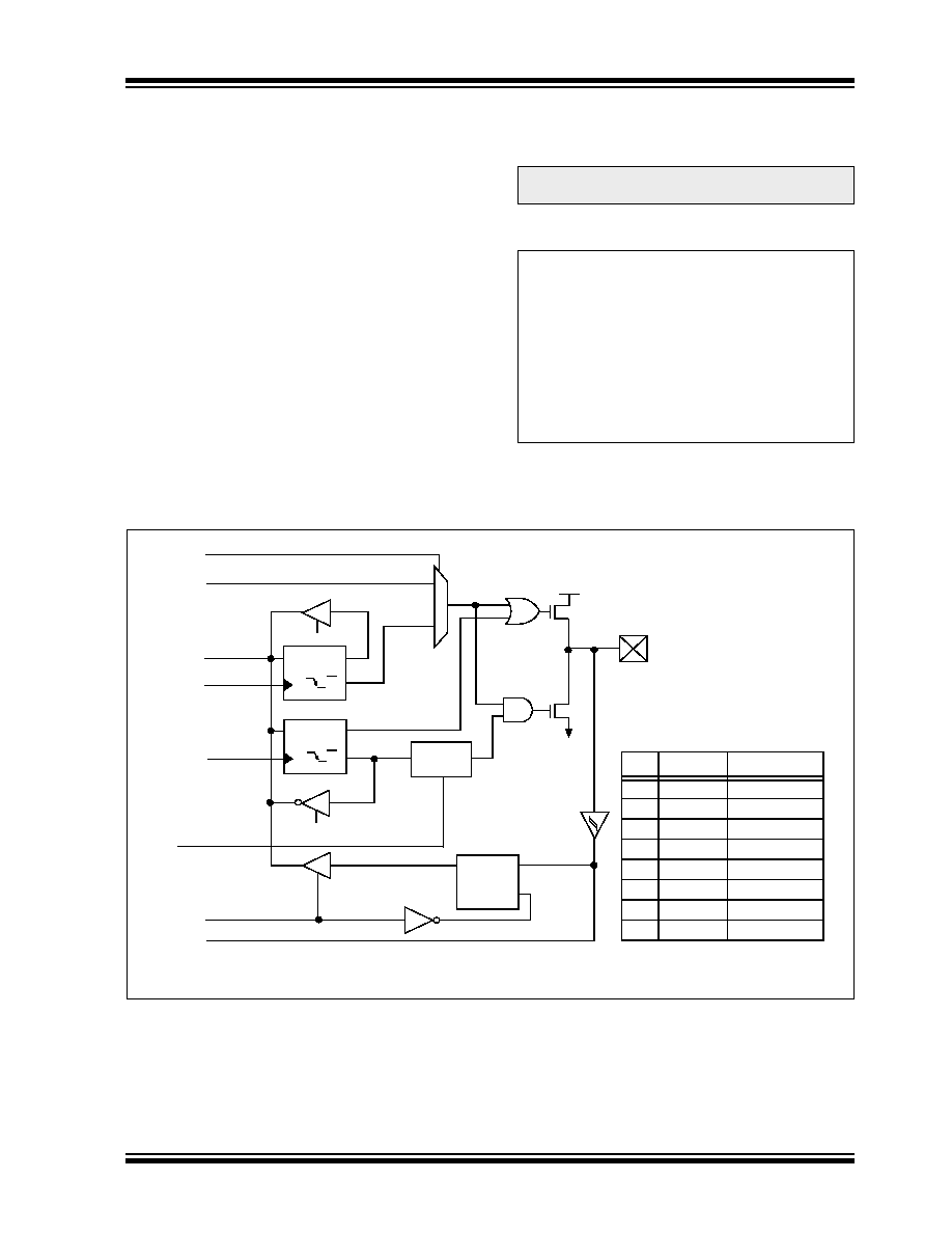
FIGURE 9-9:
PORTE BLOCK DIAGRAM IN I/O MODE
Note:
On Power-on Reset, PORTE defaults to
the system bus.
CLRF
PORTE
; Initialize PORTE by
; clearing output
; data latches
CLRF
LATE
; Alternate method
; to clear output
; data latches
MOVLW
03h
; Value used to
; initialize data
; direction
MOVWF
TRISE
; Set RE1:RE0 as inputs
; RE7:RE2 as outputs
Peripheral Out Select
Data Bus
WR LATE
WR TRISE
Data Latch
TRIS Latch
RD TRISE
Q
D
Q
CK
QD
EN
Peripheral Data Out
0
1
Q
D
Q
CK
P
N
VDD
VSS
RD PORTE
Peripheral Data In
I/O pin(1)
or
WR PORTE
RD LATE
Schmitt
Trigger
Note 1: I/O pins have diode protection to VDD and VSS.
TRIS
Override
Peripheral Enable
TRIS OVERRIDE
Pin
Override
Peripheral
RE0
Yes
External Bus
RE1
Yes
External Bus
RE2
Yes
External Bus
RE3
Yes
External Bus
RE4
Yes
External Bus
RE5
Yes
External Bus
RE6
Yes
External Bus
RE7
Yes
External Bus
发布紧急采购,3分钟左右您将得到回复。
相关PDF资料
PIC18C658T-I/L
IC MCU OTP 16KX16 CAN 68PLCC
PIC18C658T-E/L
IC MCU OTP 16KX16 CAN 68PLCC
PIC16C925T-I/L
IC MCU OTP 4KX14 LCD DVR 68PLCC
PIC12F675-E/P
IC MCU CMOS 1K FLASH W/AD 8-DIP
PIC18C858T-E/L
IC MCU OTP 16KX16 CAN 84PLCC
PIC16F636-I/SL
IC PIC MCU FLASH 2KX14 14-SOIC
PIC18LC658T-I/L
IC MCU OTP 16KX16 CAN 68PLCC
PIC18LC801T-I/L
IC MCU ROMLESS A/D PWM 84PLCC
相关代理商/技术参数
PIC18C801T-I/PT
功能描述:8位微控制器 -MCU 2MB 1536 RAM 37I/O RoHS:否 制造商:Silicon Labs 核心:8051 处理器系列:C8051F39x 数据总线宽度:8 bit 最大时钟频率:50 MHz 程序存储器大小:16 KB 数据 RAM 大小:1 KB 片上 ADC:Yes 工作电源电压:1.8 V to 3.6 V 工作温度范围:- 40 C to + 105 C 封装 / 箱体:QFN-20 安装风格:SMD/SMT
PIC18C858-E/L
功能描述:8位微控制器 -MCU 32KB 1536 RAM 68I/O RoHS:否 制造商:Silicon Labs 核心:8051 处理器系列:C8051F39x 数据总线宽度:8 bit 最大时钟频率:50 MHz 程序存储器大小:16 KB 数据 RAM 大小:1 KB 片上 ADC:Yes 工作电源电压:1.8 V to 3.6 V 工作温度范围:- 40 C to + 105 C 封装 / 箱体:QFN-20 安装风格:SMD/SMT
PIC18C858-E/PT
功能描述:8位微控制器 -MCU 32KB 1536 RAM 68I/O RoHS:否 制造商:Silicon Labs 核心:8051 处理器系列:C8051F39x 数据总线宽度:8 bit 最大时钟频率:50 MHz 程序存储器大小:16 KB 数据 RAM 大小:1 KB 片上 ADC:Yes 工作电源电压:1.8 V to 3.6 V 工作温度范围:- 40 C to + 105 C 封装 / 箱体:QFN-20 安装风格:SMD/SMT
PIC18C858EPT
制造商:MICRO CHIP 功能描述:New
PIC18C858-I/L
功能描述:8位微控制器 -MCU 32KB 1536 RAM 68I/O RoHS:否 制造商:Silicon Labs 核心:8051 处理器系列:C8051F39x 数据总线宽度:8 bit 最大时钟频率:50 MHz 程序存储器大小:16 KB 数据 RAM 大小:1 KB 片上 ADC:Yes 工作电源电压:1.8 V to 3.6 V 工作温度范围:- 40 C to + 105 C 封装 / 箱体:QFN-20 安装风格:SMD/SMT
PIC18C858-I/PT
功能描述:8位微控制器 -MCU 32KB 1536 RAM 68I/O RoHS:否 制造商:Silicon Labs 核心:8051 处理器系列:C8051F39x 数据总线宽度:8 bit 最大时钟频率:50 MHz 程序存储器大小:16 KB 数据 RAM 大小:1 KB 片上 ADC:Yes 工作电源电压:1.8 V to 3.6 V 工作温度范围:- 40 C to + 105 C 封装 / 箱体:QFN-20 安装风格:SMD/SMT
PIC18C858T-E/L
功能描述:8位微控制器 -MCU 40MHz 16K OTP RoHS:否 制造商:Silicon Labs 核心:8051 处理器系列:C8051F39x 数据总线宽度:8 bit 最大时钟频率:50 MHz 程序存储器大小:16 KB 数据 RAM 大小:1 KB 片上 ADC:Yes 工作电源电压:1.8 V to 3.6 V 工作温度范围:- 40 C to + 105 C 封装 / 箱体:QFN-20 安装风格:SMD/SMT
PIC18C858T-E/PT
功能描述:8位微控制器 -MCU 32KB 1536 RAM 68I/O RoHS:否 制造商:Silicon Labs 核心:8051 处理器系列:C8051F39x 数据总线宽度:8 bit 最大时钟频率:50 MHz 程序存储器大小:16 KB 数据 RAM 大小:1 KB 片上 ADC:Yes 工作电源电压:1.8 V to 3.6 V 工作温度范围:- 40 C to + 105 C 封装 / 箱体:QFN-20 安装风格:SMD/SMT